MechaCrypt: A Solenoid-Based Encrypted Data Transmission System
Introduction and Project Overview
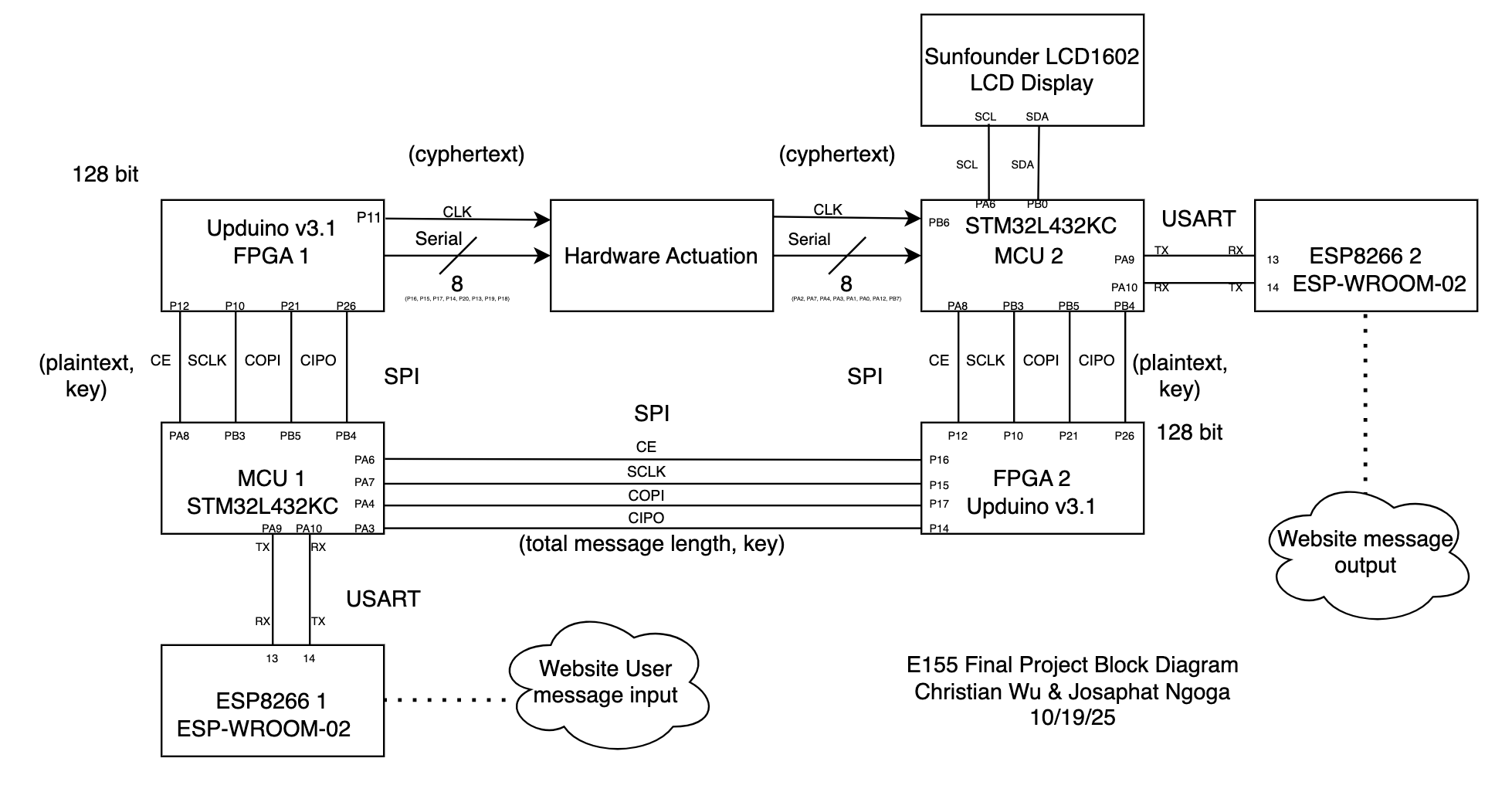
The goal of the project is to demonstrate serial data transfer through a mechanical actuation mechanism rather than traditional electrical signaling. Mechanical motion, driven by solenoids, relays, and limit switches, replaces voltage as the medium for communication across nine parallel channels, with one serving as the CLK for synchronization and eight for data bits, transmitting one byte per cycle in simplex mode. Each relay energizes a solenoid when its input is HIGH, pressing a limit switch on the receiver side to register a HIGH signal. For secure communication, the sender encrypts messages using AES-128, and the receiver decrypts the transmitted bytes to reconstruct the plaintext. Communication between sender and receiver is coordinated through a web app: the user types or uploads a message, where the ESP8266/ESP32 sends/receives a request to/from the MCU–FPGA system for encryption, transmission, decryption, and final display of the recovered message on the receiver’s web page.
FPGA Use
The project uses two FPGAs, one on each side of the communication system. Each FPGA handles AES-128 encryption and decryption while interfacing directly with the mechanical bus. The sender FPGA receives plaintext and encryption key from the MCU, encrypts it, and performs bit-banging to maintain synchronization and ensure that a complete byte is transmitted every cycle. The receiver FPGA reads each incoming byte, decrypts it, and sends the plaintext to the MCU for display. It also manages switch input synchronization through debouncing to ensure clean and reliable signal detection. The new FPGA function is highlighted below:
- Using SPRAM to store encrypted ciphertext, and then pulling from the SPRAM 8 bits at a time to transfer via hardware actuation.
The FPGAs communicate with the MCUs through SPI and interface with the mechanical bus using a custom serial bit driver that handles all data transmission and input reception. The transfer rate of the bits will be set depending on how we synchonize the receiving end. Bit transfer is handled by the clock, and we can change the clock speed to achieve synchronization, and this will in turn affect how fast we can send bits across.
FPGA Resource Usage
The FPGAs in this setup will perform AES-128 encryption and decryption, both of which rely heavily on combinational logic, resulting in high LUT usage. Most of the resources are consumed by the iterative round operations, key expansion, and storing S-box substitution tables, with additional LUTs used by the FSMs that will control the actuators and debounce switch inputs. The UPduino has built-in macros for SPI, but serial communication can also use some resources. From research on the implementation of these functions, we estimated a total of ~3500 LUTs. Since each UPDuino (iCE40UP5K) provides 5,280 logic cells, this remains within a safe utilization range. For on-board storage, only about 5 kB of the available 128 kB memory is required for S-box tables and related data. The tasks stated above are split between 2 FPGAs, therefore, we stay even further from the resource limits of the boards.
MCU Use
The project uses two MCUs, one for each side of the system. They serve as the main interface for web communication and text encoding, converting messages into byte data that the FPGA can process. MCUs are ideal for this role due to their large on-board memory, which allows them to handle larger text data. Each MCU also participates in the encryption and decryption process, managing the exchange of keys and ciphertext/plaintext with the FPGAs. Additionally, the MCUs will control all system indicators and feedback mechanisms that help monitor the efficiency of the system. The new MCU function is shown below:
- Using the TRNG to randomly generate keys for encryption. We will send these random keys to the receiver via SPI so that it can decrypt the message correctly.
Bill of Materials
| Part Name | Part Number | Quantity | Vendor | Price | Link |
|---|---|---|---|---|---|
| 12V Relay Module | SRD-12VDC-SL-C | 10 | AEDIKO | 13.20 | Link |
| 12V Solenoid | Z24G50031OJX | 9 | TEHAUX | 28.26 | Link |
| Roller Lever Arm Micro Limit Switch | KW12-3 | 10 | HiLetgo | 6.60 | Link |
| LCD Display with I2C Adapter | LCD2004 | 10 | SunFounder | 14.26 | Link |
| FPGA | Upduino v3.1 | 2 | Upduino | Stockroom | N/A |
| MCU | STM32L432KC | 2 | STM | Stockroom | N/A |
| Metal Rods | N/A | 9 | N/A | Stockroom | N/A |
| ESP8266 | ESP-WROOM-02 | 2 | Edwin Robotics | Stockroom | N/A |
| Total | $62.32 |
Project Performance Specs
We expect the toughest stage to be the mechanical bus. Synchronizing all actuators and making sure that the receiver samples at the correct time will be the biggest challenge. Since the clock is also mechanical, the whole system is susceptible to any faults from that channel. Below are the main performance specs and secondary specs to check-off to verify the process and completeness of the project:
- Main Performance Specs:
- Project Midpoint Demo Specs: At Minimum, the following must be completed:
Project Timeline & Task Allocation
- By 10/26/2025: Have the proposal and project approved and verified to begin working (Both).
- Week of 10/27/2025: Submit purchase order. Develop and test MCU-FPGA encryption module (Josaphat) and MCU driver for ASCII encoding/decoding and web requests (Chistian).
- Week of 11/03/2025: Machine and cutdown metal rods. Start assembling and testing the electronics and mechanical system. Troubleshoot annd resolve any issues errors (Both).
- Week of 11/10/2025: Develop and test MCU-FPGA decryption module (Josaphat) and MCU code for system monitoring and fault detection (Christian).
- Week of 11/17/2025: Preliminary testing of the full system. Connecting all parts and running all systems to check performance and troubleshoot errors (Both).
- Week of 11/24/2025: Begin preliminary project report. Debug if any errors are still ongoing. If complete, look at implementing some strech goals or aesthetic modificatons. (Both)
- Week of 12/01/2025: Finalize report. Perfom final system shakedown to validate all performance specs and prepare checkoff sheet. PROJECT DEMO!!! (Both)
Appendix
The appendix contains images and diagrams highlighing the full setup and other considerations to ensure the project goes as planned:
All the relevant elements defined in the description above and will be connected together following the communication protocols and setup in Figure 1 below:
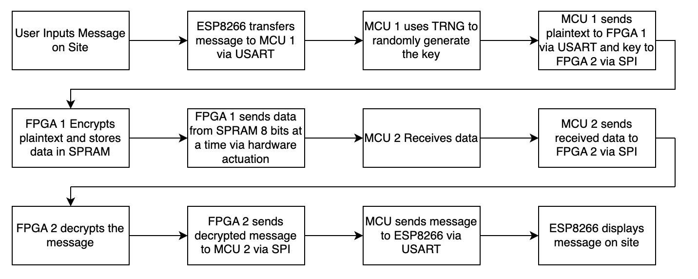
Below is also a flowchart of how messages go from the user to receiver through our project in Figure 2:
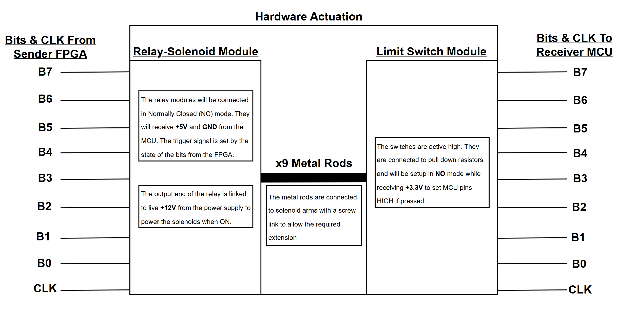
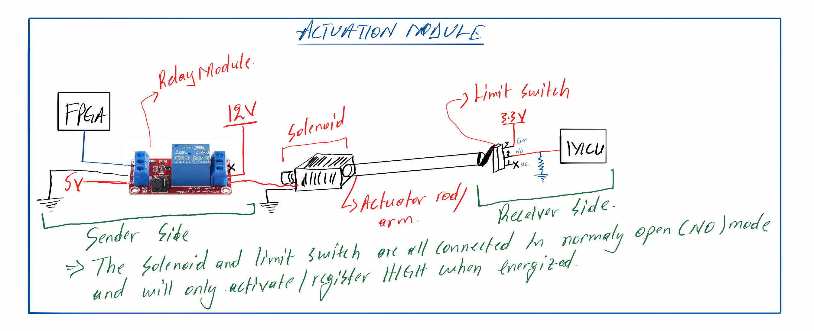
The actuation block requires different modules and setup necessary for it to work as expected. The relay module specifications show the mentioned NO and NC connection modes. Figure 3 below shows the signals as well as voltage and circuit configurations:
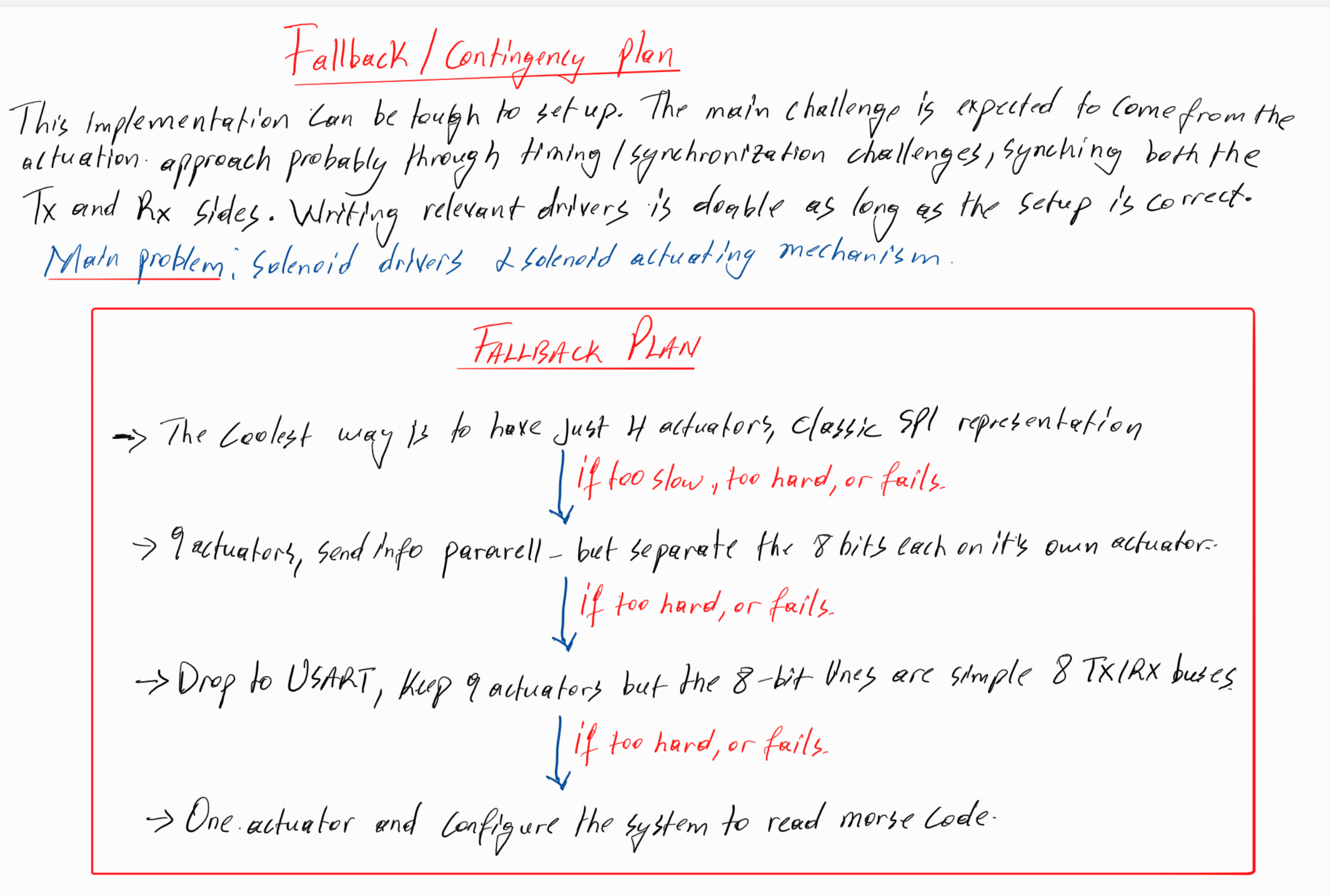
The team has a fall-back plan in case new errors and challenges come up along the way to ensure that at least the main idea of transfering encrypted data mechanically still stands.