Hardware-Accelerated AES Encryption
Introduction
AES is a symmetric encryption algorithm that uses a specific key to both encrypt and decrypt data. It is the global standard for secure data encryption and is defined in three key sizes: AES-128, AES-192, and AES-256, where the number indicates the bit length of the cipher key. A larger key size provides stronger security but requires more hardware resources. The MCU and FPGA combine to implement a hardware-accelerated version of the Advanced Encryption Standard (AES) for 128-bit data encryption. The MCU stores and provides the plaintext and cipher key, transmitted to the FPGA via the SPI interface. The FPGA performes the AES encryption according to the NIST-197 standard and then returns the resulting ciphertext to the MCU for verification. The description below ou
Encryption Overview
AES encrypts data through a sequence of sub-algorithms and transformations that repeatedly mix the key with the plaintext to produce a ciphertext that appears random and cannot be reversed without the correct key. These transformations operate on matrices of bytes, with the key itself acting as one of the main transformation matrices. The encryption process consists of four main operations:
- SubBytes(): performs a non-linear byte substitution using a 16×16 S-box lookup table of random magic numbers.
- shiftRows(): cyclically shifts the rows of the state matrix to the left by varying offsets depending on row.
- mixColumns(): transforms each column of the state matrix using Galois Field arithmetic to further diffuse the data.
- AddRoundKey(): combines the current state with a round key using a bitwise XOR operation.
Finally, these operations are repeated across multiple rounds of encryption, each using a different round key derived through an algorithm known as keyExpansion(). In the AES-128 implementation used in this application, the encryption involves 10 rounds. Each round follows the sequential: AddRoundKey → SubBytes → ShiftRows → MixColumns, with the final round (10) skipping the MixColumns step. This datapath aggregated over 10 rounds is what constitutes the full AES Encryption.
Experiment Setup and Design Overview
MCU Setup
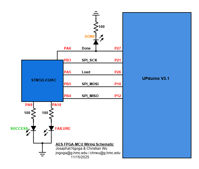
The MCU was configured to implement the SPI mode 1. It was also set up as the master with an artificial chip select signal to allow 8-bit CE-based SPI decoding on the logic analyzers. The MCU controlled the internal signals that started the SPI transactions. The MCU would set the signal load to the FPGA that prepares it to recieve inputs. The MCU then sends the cipherkey and then the plaintext and then would set load LOW to signal that all data is sent. During that period, the FPGA performs encryption and once all 10 rounds complete, the FPA sets the signal done HIGH so that the MCU prepares to receive the ciphertext.
For debugging: MCU had code that tested using standard NIST vectors. Once the cyphertext is received, it compared it to the expected cyphertext through a difference operation. If all operations yield zero, a green LED through PA9 would light up, otherwise a red LED at P10 lights up indicating that encryption didn’t work properly. This process was always triggered using the MCU reset that restarted the transactions.
FPGA Setup and Encryption Pipeline
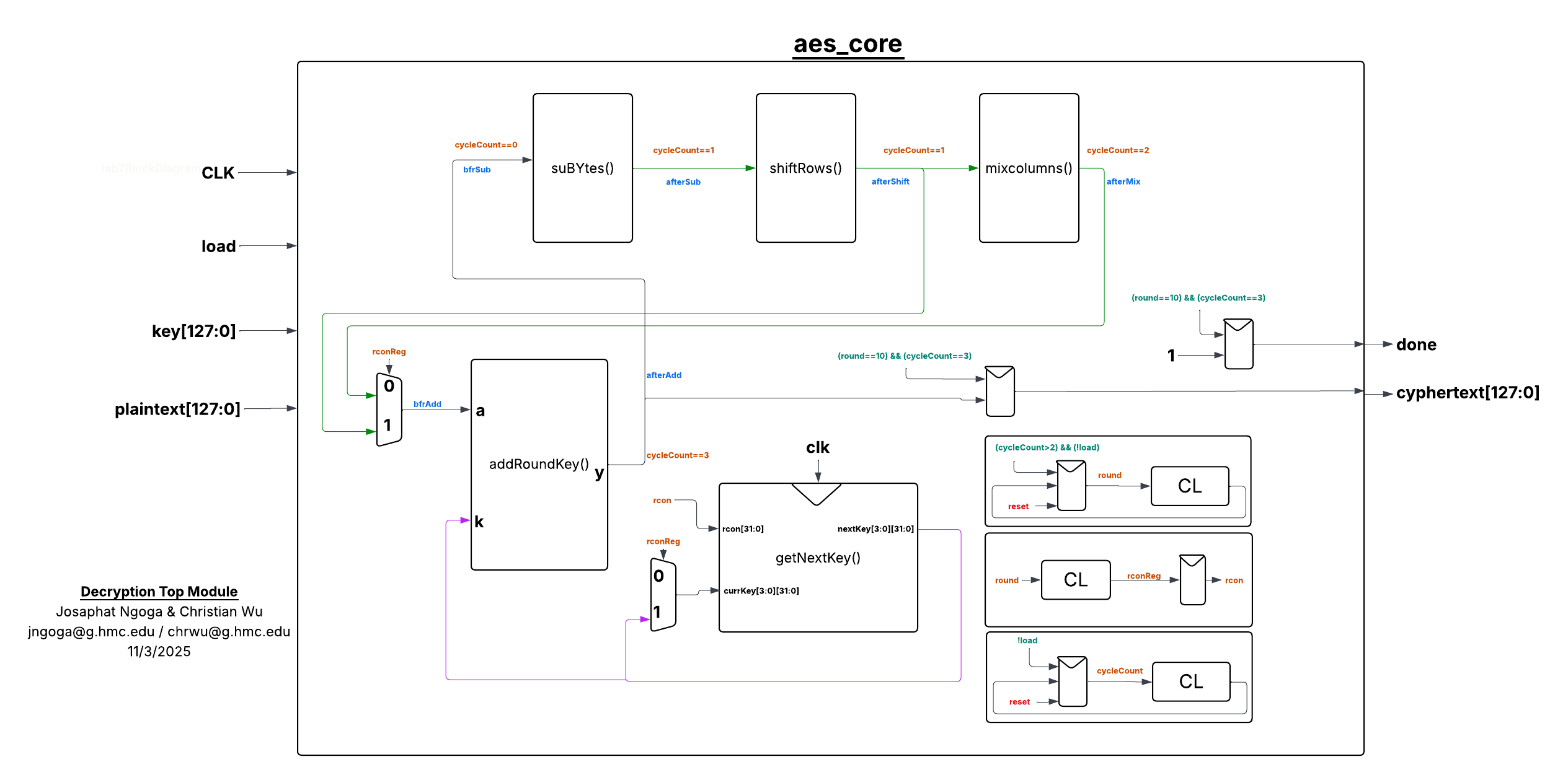
Since all encryption was done by the FPGA, we had to write SystemVerilog modules to perform the transformation operations necessary for executing the AES encryption. A lot of these operations required heavy resource usage as operations such as key expansion are applied across a 128-bit word. This would always run the risk of exhausting LUTs and other FPGA resources. Therefore we had to take into account how the encryption logic is synthesized to ensure the implied hardware isn’t too heavy for the FPGA. The subBytes() lookup table was loaded into the FPGA embedded block RAMs (EBR) which have the ability to store files upto 128kB. To ensure it is mapped properly to the EBRs, we used a clocked version of the AES byte substitution algorithm named sbox_sync(). This module could only parse an 8-bit word so in subBytes(), it was called 16 times to parse the full 128-bit word. The shiftRows() module performed some row permutation by rotating the 4 rows: row 0 was kept as is, row 1 was shifted left by 1, row 2 by 2, and row 3 by 3. After row permutation, mixColumns() treats each state as a four-byte vector and performs matrix multiplication (Galois field operations) on the bytes in a column withinin \(GF(2^8)\) followed by XOR operations to handle overflows. Next up is the addRoundKey() that performs XOR operations between the 128-bit word and the 128-bit key. Finally, the module getNextKey() which performed the key expansion part of AES which receives a 128-bit key value and the tound constant, rcon, which is a series of 4-byte words used in the key schedule to create the sub-keys for each encryption round. The module would determine the key for the next round following the implementation and pseudocode provided in the standards document.
Using a synchronized sbox meant that it takes multiple cycles per round to process the data sequentially and safely propagate signals through the combinational logic. Therefore we used cycleCountto basically set when to take inputs, when to latch outputs and when to move to the next rounds. The cycle count was also to help account for the single cycle delay caused by subBytes(). Without it, the datapath would race and try to perform key operations before byte substitution stabilizes.
All the submodules described above were combined in a module named aes_core() whose job was implement the encryption datapath. The datapath followed the structure described in the AES Overview section above. The module took in the load signal that is asserted by the MCU after sending the plaintext and key, then initiated the process. The FPGA would continously reset/update internal signals as long as load was HIGH. For round 0, the plaintext is XORed with the key and the result is passed on to the next rounds. In rounds 1 to 9, the key is updated each round alongside the the input to the datapath. This input is represented in the code as state as it hold the intermediate states of the data in-between rounds. After round 10, the done signal is asserted to prepare the MCU to receive the cyphertext.
To run the setup, we implemented the aes() module that prompts both aes_core() and the aes_spi() module that executes SPI communication between both the MCU and the FPGA. Since data is received by the FPGA based on SCK from the FPGA, we added a synchronizer that ensures the load signal referenced by the FPGA for encryption, is latched on the rising edge of the FPGA internal clock (HSOSC/clk) instead of the SPI clock domain. This eliminated any potential synchronization issues where encryption would be randomly true/false depending on the data latched. The connection and signals between these modules is shown in Figure 1.
Design Implementation
The modules to enforce the AES encryption and those that control the respective encryption transformation algorithms were written in SystemVerilog to run on the FPGA. To ensure proper communication and signal control between the MCU and FPGA, all signals followed the hierachy in the block diagram below:
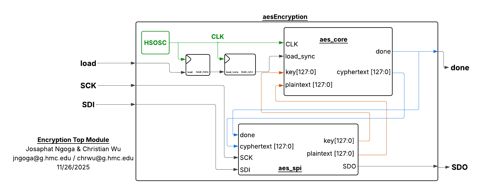
aes_core() involves multiple blocks and enabler logic that manages the flow of signals and data through the different transformations within the datapath as shown in Figure 2 below:
To ensure proper functionality and communication, the full setup is installed on the development board. The board used already had DIP switches that connect specific MCU pins to specific FPGA pins which reduces the need for crossing wires. Other necessary signals like the debugging LEDs are setup on a side breadboard. The complete setup is shown in the following schematic: