MCU Design
Introduction
This project consists of two MCUs, one for the sender end, and one for the receiver end. For each MCU, we will describe each peripheral that we integrate it, how communication is established with the MCU, and what data is sent.
Sender MCU Design
For the sender MCU, it will utilize TRNG to generate random keys, it will connect to the sender FPGA where encryption occurs and it will be connected to a ESP8266 where user inputs occur. Below, we will describe in detail how this was implemented.
TRNG Implementation
The STM32L432KC MCU has a built in True Random Number Generator (TRNG). The TRNG generates 32 random bits, so we need to read it four times to generate 128 random bits, which equates to a random key that is used for AES-128 encryption. The code is designed so that when the sender sends a message over the website UI, the website calculates how many 128 bit blocks are required to send over the message. The MCU code will then generate a random 128 bit key for each of the message blocks and store it on an array in the MCU to be sent to the sender and receiver FPGA.
Connection with Sender FPGA
The STM32 MCU interacts with the sender FPGA via SPI, which is the same as the way it was set up in lab 7. The data that is sent over to the FPGA is the plaintext and its randomly generated key. Given that our system is built to be able to send multiple 128 bit blocks, we need to know when the FPGA has encrypted a block and is ready to receive the next block and encrypt it. This is achieved by the FPGA sending a done signal to the MCU so that the MCU will send over the next set of plaintext and key. The very first block sending of the program is triggered by the user when hitting the send button on the website, all subsequent block sending is based on the done signal sent by the FPGA.
In terms of hardware, in order to save pins, we will be using the same output pins for the SPI connections between the MCU and both the sender and receiver FPGA. In other words, it means that SCK, COPI, and CIPO are the same MCU pins wired to both FPGAs. In order for the two FPGAs to not read the wrong data, we have a separate chip enable wire going to each of the FPGAs. That way, each FPGA knows when the data sent over SPI is meant for it.
ESP8266 Integration
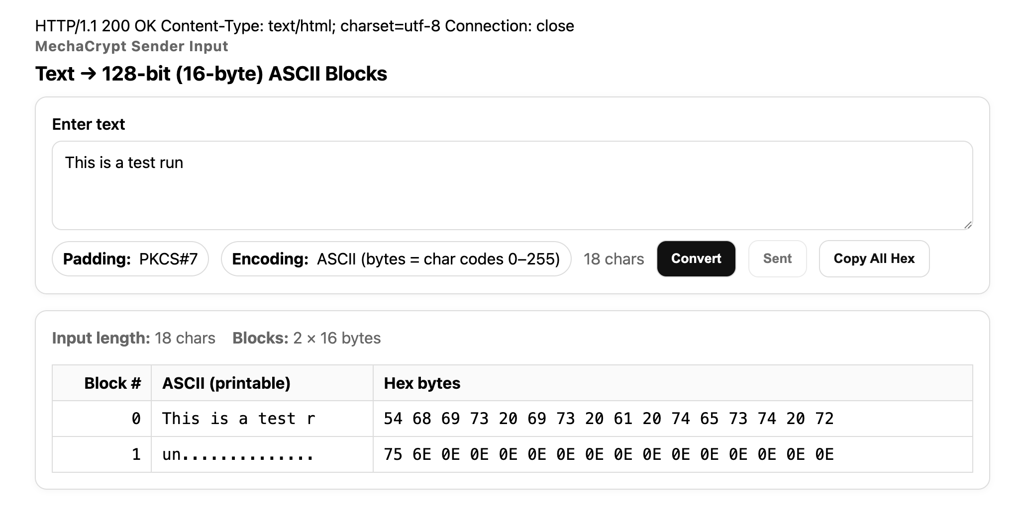
The sender MCU uses an ESP8266 for its messaging UI for both the sender and receiver. THe MCU and ESP8266 connect via USART, which is the same as we have done with previous labs. On the sender side, the user will input their desired message. They can then click the convert button, which will show them how many blocks of data are gonna be sent, as well as the data that will be sent. The data will be in hex, which is the ASCII equivalent of the text in hex form, which is what we need to input into the FPGA. Since the FPGA uses AES-128 encryption, we need to ensure that each block of text is 128 bits long, even if the message is not that long. To do this, we can use padding, which will fill the remainder of the 128 bit block. We used PKCS #7 padding, which will fill in the remainding bytes needed in the block with the number of bytes that it is filling in. 128 bit blocks are equivalent to 16 bytes, so if we only use 8 bytes worth of text in the block, it will fill the remaining 8 bytes with 0x08. Then, the user can click send, which will start the whole sending transaction for the system. Below is a sample image of what the website UI looks like for the user:
Receiver MCU Design
For the receiver MCU, it connects with the receiver FPGA for decryption, it connects with the ESP8266 for the receiver end website, it connects with the mechanical actuation system to receive the encrypted ciphertext, and it connects with an LCD display to show live progress of the message transfer.
Connection with Receiver FPGA
The receiver MCU interacts with the receiver FPGA via SPI, which is the same as the way it was set up in lab 7. The FPGA will send the decypted plaintext to the MCU via SPI.
ESP8266 Integration
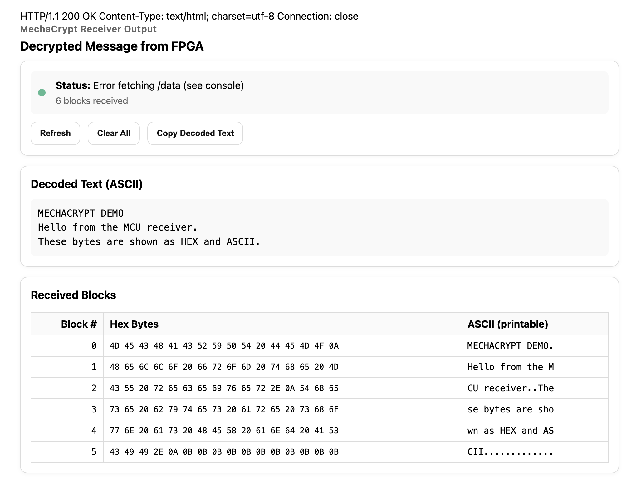
The receiver end ESP8266 displays the decrypted text to the receiver end user, which should match what the sender sent originally. Given that the mechanical system takes a while to send the data, the receiver end website will display one block at a time until all the blocks have arrived to the receiver side and have been decrypted. The receiver end website UI is built to be similar to the sender UI to demonstrate that encryption and decryption worked correctly, showing each individual 128-bit block of data as well as the full message. Below is a sample image of what the receiver end website UI looks like for the user:
LCD Display Integration
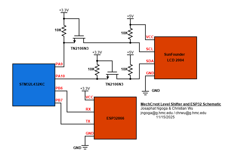
In order to track how much data has been sent over and how close we are to the full message transaction being complete, we have implemented the use of an LCD Display. We purchased an LCD Display with an I2C adapter, meaning that it will only require 2 MCU pins instead of 8. This saves up a lot of pins, given that the MCU also needs to connect to the ESP8266, the receiver FPGA, and the mechanical actuation system. To drive the LCD display and the I2C adapter, we need a 5V source, which is provided by our motherboard. For the I2C adapter to register a high value, it needs at least \(0.7 V_{DD}\), which is 3.5 V. However, our STM32 pins only output 3.3 V. Thus, we need to use a level shifter, so that the I2C adapter can properly read low and high values. Below is a schematic of our level shifter implementation for our display:
To run the actual display, we were able to use files provided by the manufacturer, which had functions made to control the display. However, this file was in C++, so we had to convert it to C. Once that was done, we were able to initialize I2C on our MCU and display a progress bar on our display. Below is a video demonstrating what the progress tracking would look like: