FPGA Design
Introduction
This project consists of two FPGAs, one for the sender end, and one for the receiver end. For each FPGA we describe the different modules involved, how they influence and affect the system overall and describe any connections between the FPGAs and either of the MCUs
Sender FPGA Design
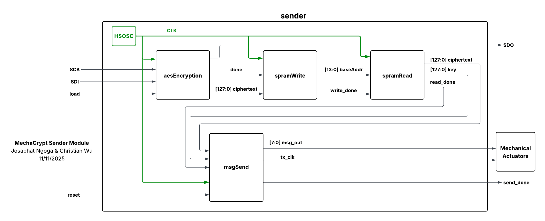
The main goal of the sender FPGA was to receive data from the MCU, encrypt it and proceed to send it over by triggering the merchanical system effectively. All relevant modules are described in the chapters below.
AES Encryption Module
This module talks to the MCU via SPI. The MCU communicates to this module by sending a chipselect signal that prepares this module to receive the plaintext and the generated key. The SPI implementation on the FPGA is a shift register that continously shifts data in from the MCU MOSI or out through the MCU MISO. The module also proceeds to encrypt the given ciphertext and will return the ciphertext, the key, and a signal, done, indicating that encryption is completed. Information about encryption can be found in AES Encryption Overview webpage.
SPRAM Implementation
We implemented on-chip SPRAM (Single-Port RAM) to temporarily store the ciphertext within the FPGA, effectively reducing reliance on and potential exhaustion of other limited on-board memory resources. SPRAM offers fast access speeds and a straightforward interface for both read and write operations. Lattice provides the dedicated hardware macro SB_SPRAM256KA for this purpose, enabling efficient data buffering between the AES core and the external communication modules. Each iCE40UP5K FPGA includes four SPRAM blocks, each providing 16K × 16 bits (256 Kb) of storage. This translates to a total of 1 Mbit (128 KB) of available SPRAM, capable of holding up to 8,192 AES ciphertext blocks (each 128 bits). In our design, writing and reading operations are performed sequentially using the same base_addr indexing scheme that was used to store each ciphertext, ensuring proper data reconstruction and alignment during retrieval.
Actuation Module
This module’s primary purpose is to send any desired message and/or data through the mechanical actuators. We used it to send the ciphertext and key to the other side. Given a specific FPGA clock frequency, CLK_FREQ, we can set our desired transfer frequency TX_FREQ which is implemented using a specific clock divider that ensures the ourput clock matches the desired frequency. THe module splices the 256 bits into 32 blocks, each carrrying 1 byte. The byte lines are activated on the rising edge of tx_clk and closed on the falling edge. This was designeed to ensure the FPGA on the other can properly sample the inputs and that we can debounce effectively.
Sender Module
This module combines all the modules above to ensure they are connected and communicate properly. It instantiates the FPGA main clock and is able to connect and communicate to everything effectively.
Receiver FPGA Design
The receiver FPGA received the bytes from the actuators, concatenated them to reconstruct the cyphertext and the key, sent them directly to the decryption module which executed decryption and would send the results to the MCU via SPI.
Byte Receiving Module
On the rising edge of tx_clk, the module waits a short time and then samples the signal lines to read the inputs. It has a variable TOTAL_BYTES that defined the number of bytes it is expected to receive. once done, it would concatenate everything and output the the cyphertext and the key so they can be used by the decryption module. It had a custom SPI implementation that sent the received data to the MCU for debugging purposes. It was so that we can check and see if the interpreted data is exactly what we wanted.
Decryption Module
This module receives the key and cyphertext from the byte receiving module, executes decryption, and sends the results to the MCU via a custom SPI interface. Information about decryption and this module implementation can be found in AES Decryption Overview webpage.
Reciever Module
This module combines all the modules above to ensure they are connected and communicate properly. It instantiates the FPGA main clock and is able to connect and communicate to everything effectively.